April 1, 2014 – March 31, 2015
High efficiency n-IBC cell and module technology in the Netherlands
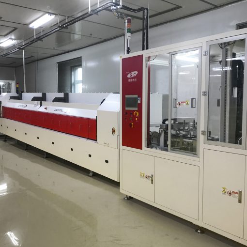
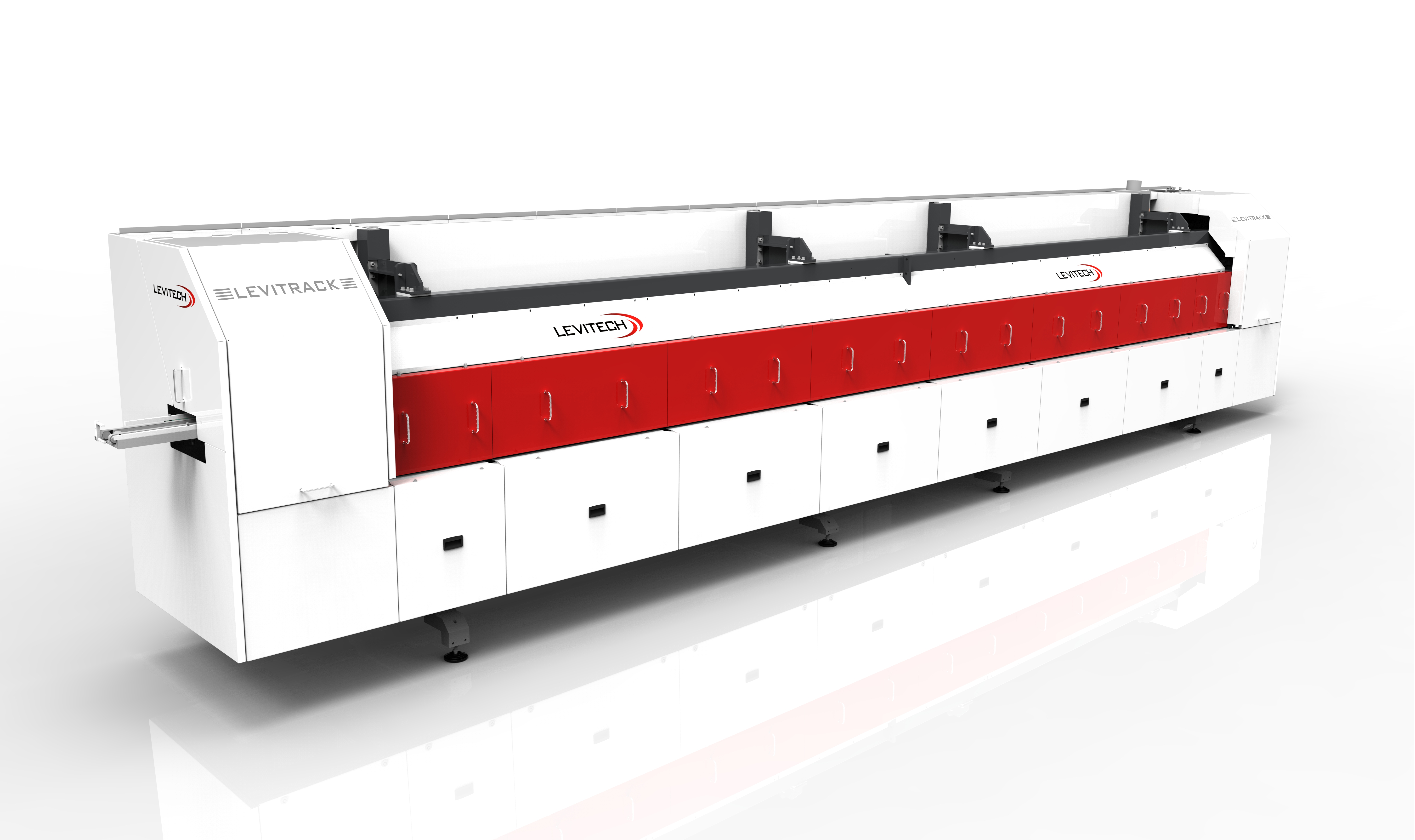
The growth of the PV market has been spectacular in the last years. At the same time a significant shift occurred in production location from Europe to Asia while equipment manufacturing has largely remained in Europe. To support Dutch equipment manufacturers to realize and maintain a strong position in the Photovoltaic sector, the High-Tech “IBChampion” consortium led by Levitech B.V. is determined to develop a high-efficiency Interdigitated Back Contact (IBC) solar cell as a natural up-grade of the n-PASHA solar cell which is currently mass produced at Yingli Solar using technology and equipment from Dutch OEM. The collaborating parties comprise further of Dutch equipment manufacturers Tempress, ASM, Roth & Rau B.V. and Eurotron; and the knowledge centres Energy research Centre of the Netherlands (ECN), Delft University of Technology (TUD) and the Eindhoven University of Technology (TU/e).
The targeted efficiency of the IBC cell is 22 – 23% based on a 6 inch wafer. With this cell, the consortium aims to demonstrate the feasibility of a full-sized module with a 20.5 – 21.5% full-area module efficiency. The result will be achieved with a process that only adds 1 to 4 extra steps to the already commercialized n-PASHA process. With this cost-effective cell and module technology, the consortium develops a low-cost alternative to Sunpower’s IBC module with an efficiency of 21.5%.
The main targeted innovations of “IBChampion” are:
- A low-cost IBC cell concept based on ECN patents that which features wide contact regions for both polarities without loss in cell performance and therefore making easy module integration possible;
- A rear side contact design that will reduce the metal consumption (lower €/Wp) and will enable easy module integration;
- A process sequence with a limited number of process steps and comparable to the n-PASHA process and therefore making it possible to harmoniously introduce the technology in current production facilities;
- Novel and potentially better surface passivation schemes based on ALD and CVD;
- New junction formation technologies with better cost structure;
- New patterning and contacting schemes to reduce the processing cost;
- Foil based interconnection technology enabling the use of large wafers and high throughput.
The project will run for 2 years, starting April 2014. The technology and processes will be integrated into the conceptual cell and module designs at minimal €/Wp cost. This optimization will be supported by device simulations and cost of ownership calculations.